
Asset Locating System for Electronics Manufacturing

Modern electronics manufacturing demands instant visibility. WISER’s asset locating system for electronics manufacturing delivers real-time tracking of WIP, tools, PCBAs, semiconductors, and subassemblies with sub-meter accuracy. The system uses ultra-wideband technology and auto calibrating wireless mesh network to locate every tagged asset across your facility. With us, operators stop searching, and production keeps moving.

Precision Tracking Built for Non-Linear Electronics Manufacturing

WISER’s asset locating system for electronics manufacturing tracks moving parts, tools, and assemblies in real time without relying on fixed workflows or manual scans. It maintains accuracy in metal-rich, signal-hostile environments where RFID and BLE systems fail.

This innovative functionality allows facility teams to gain reliable, real-time visibility without disrupting their existing production flow. This same resilience makes it ideal for semiconductor facilities, where wafers, carriers, and tools move through variable process steps across multiple cleanroom zones.

WIP Asset Locating for Electronics & Automotive Subassemblies ​
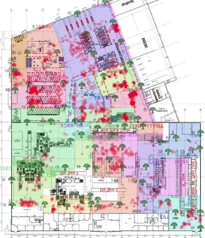
Electronics subassembly lines demand total visibility of in-progress materials, tools, and components – especially when workflows shift or bottlenecks appear without warning. Some of the most common applications include:

  • PCB Assembly Zones: Track boards through soldering, inspection, and rework without manual scans
  • Automotive Electronics Subassembly: Monitor harnesses, sensors, and modules across multiple lines
  • Tool Tracking: Ensure location and readiness of shared tools, gauges, and fixtures
  • Quality and Calibration Areas: Maintain full visibility and automatic audit trails for assets under inspection, calibration, or quality hold
  • WIP Staging and Buffer Zones: Locate partial builds and prevent slowdowns caused by misplaced work
  • Semiconductor Fabrication and Packaging: Track wafers, carriers, and process tools across cleanroom zones for precise, contamination-safe visibility

By bringing real-time location data into these key processes, manufacturers reduce search time, tighten traceability, and avoid delays that compromise delivery schedules.


See Why Electronics Manufacturers Trust WISER

Talk to Expert

Electronics and automotive subassembly teams use WISER’s asset locating system for real-time visibility, fewer delays, and complete control of their WIP. If you’re struggling to track assets through PCB assembly, semiconductor fabrication, rework stations, or high-mix production lines.

Schedule a demo or contact our team to find out how WISER can support your facility’s specific workflow.

Electronics WIP Asset Locating Systems FAQ

Learn more about WISER’s asset locating systems through our frequently asked questions below.
Can WISER’s asset locating system for electronics manufacturing track small items like PCB totes, bins, or trays?

Yes! Our system tracks small, high-volume containers, including PCB trays, totes, and bins with compact, low-profile tags for electronics environments.

How does the system handle multi-floor or complex facility layouts?

WISER’s asset locating system for electronics manufacturing uses a wireless mesh that scales across buildings, floors, and zones without losing accuracy or requiring fixed pathways.

What kind of maintenance do the tracking tags require?

Tags are maintenance-free for years. Battery life varies by update rate, but most electronics and WIP applications run for several years without replacement.

Can I integrate this with our existing ERP or MES?

Yes. WISER’s open API connects with ERP, MES, or quality systems to sync asset location with your existing production data.

Is the system suitable for ESD-sensitive environments?

Absolutely. Our electronics WIP asset locating system includes tag and mounting options that are compatible with ESD protocols and cleanroom use.

Is WISER’s system suitable for semiconductor cleanrooms?

Yes. WISER’s ultra-wideband system operates reliably in semiconductor environments with cleanroom-compliant, ESD-safe tags and minimal infrastructure impact.